
在VHDL中实现简单的双端口块ram
我一直试图在VHDL中实现一个简单的双端口块RAM,但在仿真中没有产生预期的结果。以下是代码:
library IEEE;
use IEEE.std_logic_1164.all;
use IEEE.std_logic_unsigned.all;

entity rams is
generic ( g_adress_width: integer:= 18;
          g_ram_size: integer:= 1000
        );
 port(
    clka : in std_logic;
    clkb : in std_logic;
    wea : in std_logic;
    web : in std_logic;
    addra : in std_logic_vector(g_adress_width-1 downto 0);
    addrb : in std_logic_vector(g_adress_width-1 downto 0);
    dia : in std_logic_vector(15 downto 0);
    dib : in std_logic_vector(15 downto 0);
    doa : out std_logic_vector(15 downto 0);
    dob : out std_logic_vector(15 downto 0));
end rams;
architecture syn of rams is
    type ram_type is array (g_ram_size-1 downto 0) of std_logic_vector(15 downto 0);
     signal RAM : ram_type;
begin
 process (CLKA)
 begin
    if CLKA'event and CLKA = '1' then
            DOA <= RAM(conv_integer(ADDRA));
            if WEA = '1' then --always 0
                RAM(conv_integer(ADDRA)) <= DIA; --does not execute
        end if;
    end if;
 end process;

 process (CLKB)
 begin
 if CLKB'event and CLKB = '1' then
        DOB <= RAM(conv_integer(ADDRB));
        if WEB = '1' then
            RAM(conv_integer(ADDRB)) <= DIB;
    end if;
 end if;

end process;
end syn;
下面是模拟:
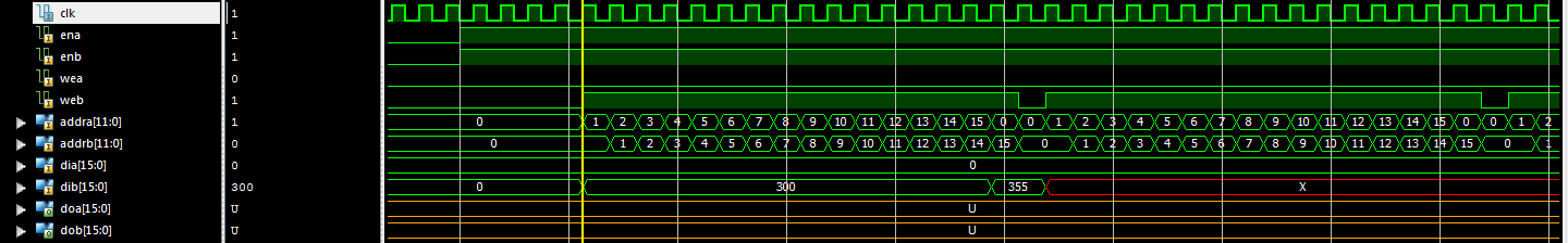
clka和clkb都连接到同一个时钟。我给dib一些任意值(无符号300和355)。
基本上,doa总是在读取,所以我希望它是未定义的,直到有东西用dib写到那些块ram地址,但是它总是显示未定义的值。
我希望doa在addra再次0岁时阅读300,当addra 15岁时阅读355。类似的情况如下(请原谅我的绘画技巧):
如果有人能指出我所做的错事的正确方向,我将不胜感激。谢谢。
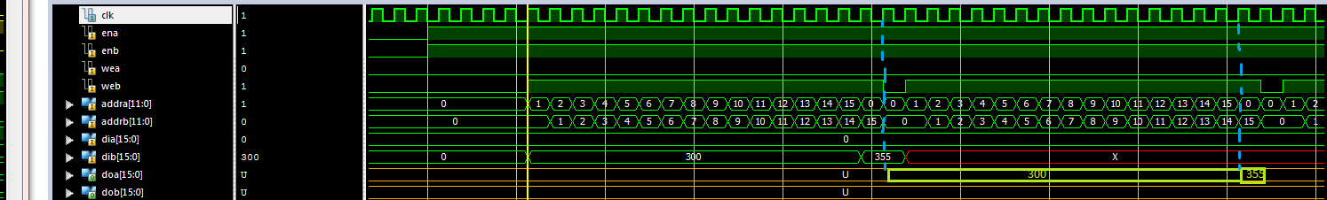
编辑:对代码进行了修改,现在它可以工作了(多亏了Paebbels解决方案):
     signal RAM : ram_type;
begin
 process (CLKA)
 begin
    if CLKA'event and CLKA = '1' then
            DOA <= RAM(to_integer(unsigned(ADDRA)));
            if WEA = '1' then --always 0
                    RAM(to_integer(unsigned(ADDRA))) <= DIA; --does not happen
        end if;

    end if;

    if CLKA'event and CLKA = '1' then
        DOB <= RAM(to_integer(unsigned(ADDRB)));
        if WEB = '1' then
            RAM(to_integer(unsigned(ADDRB))) <= DIB;
    end if;
 end if;

 end process;
end syn; 回答 1
Stack Overflow用户
发布于 2018-05-31 09:28:02
这种对双时钟RAM的描述是错误的。您需要使用以下两种方法:
- 有两个时钟的进程,或
- 共享变量。
使用一个信号和两个进程是不正确的。它在一个信号上创建多个驱动器。这反过来又会造成多个源问题。虽然您的模拟工作正常,但由于用户定义的数组类型中的解析类型std_logic_vector,合成将失败。
此外,为了允许BlockRAM的推断,您需要在VHDL代码中表示BlockRAM的内部结构。这意味着您需要在地址路径上添加管道寄存器。
您应该阅读UG901 - Vivado合成指南并搜索"RAM编码技术“。
此外,您应该使用包numeric_std而不是std_logic_unsigned,后者不是一个正式的IEEE包。
在PoC-图书馆:PoC.mem.ocram.tdp中可以找到一个工作的真双端口(TDP) PoC.mem.ocram.tdp实现。这一实施还将适用于Altera/Intel FPGA和格子FPGA。
    -- RAM can be inferred correctly only if '-use_new_parser yes' is enabled in XST options
    subtype word_t is std_logic_vector(D_BITS - 1 downto 0);
    type    ram_t  is array(0 to DEPTH - 1) of word_t;

    signal ram          : ram_t;
    signal a1_reg       : unsigned(A_BITS-1 downto 0);
    signal a2_reg       : unsigned(A_BITS-1 downto 0);

begin

    process (clk1, clk2)
    begin   -- process
        if rising_edge(clk1) then
            if ce1 = '1' then
                if we1 = '1' then
                    ram(to_integer(a1)) <= d1;
                end if;

                a1_reg <= a1;
            end if;
        end if;

        if rising_edge(clk2) then
            if ce2 = '1' then
                if we2 = '1' then
                    ram(to_integer(a2)) <= d2;
                end if;

                a2_reg <= a2;
            end if;
        end if;
    end process;

    q1 <= (others => 'X') when SIMULATION and is_x(std_logic_vector(a1_reg)) else
                ram(to_integer(a1_reg));        -- returns new data
    q2 <= (others => 'X') when SIMULATION and is_x(std_logic_vector(a2_reg)) else
ram(to_integer(a2_reg)); -- returns new datahttps://stackoverflow.com/questions/50620480
复制相似问题
腾讯云开发者

Copyright © 2013 - 2026 Tencent Cloud. All Rights Reserved. 腾讯云 版权所有
深圳市腾讯计算机系统有限公司 ICP备案/许可证号:粤B2-20090059 ![]() 粤公网安备44030502008569号
粤公网安备44030502008569号
腾讯云计算(北京)有限责任公司 京ICP证150476号 | 京ICP备11018762号