
输入和输出端口的行为是否像触发器?(VHDL)
VHDL中的输入和输出端口是否像触发器,即它们是在时钟上升或下降的边缘上更新的?这里是我的意思的一个例子。
entity main is
    port(
        clk : in std_logic; -- FPGA clock
        x : in std_logic; -- input signal
        y : out std_logic -- sampled input signal
    );
end entity main;

architecture RTL of main is
    signal y_q : std_logic;
begin

    y <= y_q; -- set the output

    copy : process(clk, x) is
        variable y_d : std_logic;
    begin
        y_d := x; -- continuously sample x
        if rising_edge(clk) then -- synchronous logic
            y_q <= y_d; -- update flip-flop
        end if;
    end process copy;

end architecture RTL;上面的程序简单地对输入信号x进行采样,并将其发送到输出y。信号y_q是采样输入信号x,而采样在时钟clk的每一个上升边缘上。然而,我对y信号感到困惑--该信号与y_q完全相同,还是延迟了一个时钟周期?
回答 3
Stack Overflow用户
发布于 2017-11-20 19:48:23
y <= y_q只是“连接”y到y_q。没有额外的逻辑暗示,所以没有延迟。
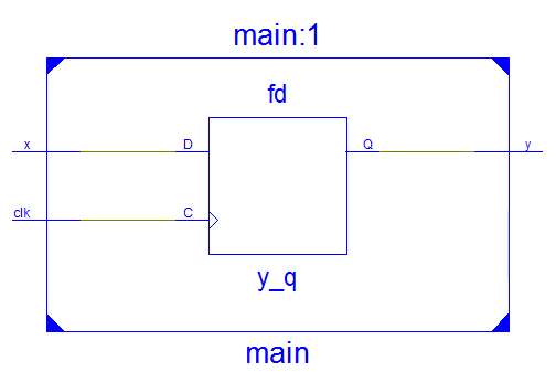
或者,您只需查看为该模块生成的RTL!下面的截图来自Xilinx。("fd“是D型触发器的Xilinx名称。)
Stack Overflow用户
发布于 2017-11-21 09:39:47
因为你问过。下面的代码被Intel/Altera和Xilinx合成所接受。
entity main is
    port(
        clk : in std_logic; -- FPGA clock
        x : in std_logic; -- input signal
        y : out std_logic -- sampled input signal
    );
end entity main;

architecture RTL of main is begin
    y <= x when rising_edge(clk);
end architecture RTL;是的,你可以使用when。你只是不能在2008年之前的过程中使用它。
Stack Overflow用户
发布于 2017-12-14 07:08:18
至于你的问题,信号y和信号y_q一样吗,答案是肯定的。Y <= y_q;是来自任何进程的并发赋值,它只是说这两个信号y和y_q应该连接在一起,所以它们当然是相同的。
您不应该以这种方式编写寄存器,尽管您的代码在逻辑上似乎是正确的。您可以查看xilinx用户指南,它将告诉您如何描述几种寄存器。
https://stackoverflow.com/questions/47399730
复制相似问题
腾讯云开发者

Copyright © 2013 - 2026 Tencent Cloud. All Rights Reserved. 腾讯云 版权所有
深圳市腾讯计算机系统有限公司 ICP备案/许可证号:粤B2-20090059 ![]() 粤公网安备44030502008569号
粤公网安备44030502008569号
腾讯云计算(北京)有限责任公司 京ICP证150476号 | 京ICP备11018762号