
当输出重叠时在输出上卡住的种类。
我对verilog非常陌生。这就是我的问题:
用16位寄存器实现16位ALU。该项目应满足以下要求。 1.设计一个16 bitALU :设计一个以X作为输入的16位ALU (例如。( A,B)并且产生一个16位的result.The ALU应该执行以下功能。ALU和逻辑的最少5次操作。 2.设计了一个16x16位寄存器文件。 3.设计了控制单元。
所以我的计划是做一堆模块,在每个模块中都有操作。然后我把它收集在实验台上。但问题是现在。输出似乎重叠,变成红色和x。
这是我的添加模块。
module Add(A,B,Y,S,clk,enb);
  parameter BITS=8;
  input clk,enb;
  input [BITS - 5:0] S;
  input [BITS - 1:0] A ,B;
  output [BITS - 1:0] Y;
  reg [BITS - 1:0] Y;

  always @(posedge clk)
  begin
  if
    ((enb==1) || (S == 000))
  begin
   assign Y = A + B;

  end
  end

endmodule
Tolak模(减模)
module Tolak(A,B,Y,S,clk,enb);
  parameter BITS=8;
  input clk,enb;
  input [BITS - 5:0] S;
  input [BITS - 1:0] A ,B;
  output [BITS - 1:0] Y;
  reg [BITS - 1:0] Y;

   always @(posedge clk)
begin
  if
    ((enb==1) || (S == 010))
  begin
  assign Y = A - B;

  end
  end
endmodule
Darab模(乘法模)
module Darab(A,B,Y,S,clk,enb);
  parameter BITS=8;
  input clk,enb;
  input [BITS - 5:0] S;
  input [BITS - 1:0] A ,B;
  output [BITS - 1:0] Y;
  reg [BITS - 1:0] Y;

  always @(posedge clk)
    begin
  if
    ((enb==1) || (S == 011))
begin
     assign Y = A * B;
  end
  end

endmodule
GateOr模块
module GateOr(A,B,Y,S,clk,enb);
  parameter BITS=16;
  input clk,enb;
  input [BITS - 14:0] S;
  input [BITS - 1:0] A ,B;
  output [BITS - 1:0] Y;
  reg [BITS - 1:0] Y;

  always @(posedge clk)
  begin
  if
    ((enb==1) || (S == 011))
  begin
   assign Y = A | B ;

  end
  end

endmodule
GateAnd模块
module GateAnd(A,B,Y,S,clk,enb);
  parameter BITS=16;
  input clk,enb;
  input [BITS - 14:0] S;
  input [BITS - 1:0] A ,B;
  output [BITS - 1:0] Y;
  reg [BITS - 1:0] Y;

  always @(posedge clk)
begin
  if
    ((enb==1) || (S == 100))
  begin
  assign Y = A & B;

  end
end

endmodule
这是我的测试台
module Maintb ();
parameter SIZE=8;
reg clk, enb ;
reg [SIZE-6:0] S;
reg[SIZE-1:0] A,B;
wire[SIZE-1:0] Y;

initial
begin
    clk = 1'b0; enb = 1'b0;
end
// generate clock
always
begin
    #(10) clk = !clk;
end
  always begin
    //#(10);
    #10; enb = 1'b1; A=00000001; B=00000000; S=000; //add
    #(10); enb = 1'b0;
    #10; enb = 1'b1; A=00000001; B=00000000; S=001; //tolak
    #(10); enb = 1'b0;
    #10; enb = 1'b1; A=00000001; B=00000000; S=010; //darab
    #(10); enb = 1'b0;
    #10; enb = 1'b1; A=00000001; B=00000000; S=011; //or
    #(10); enb = 1'b0;
    #10; enb = 1'b1; A=00000001; B=00000000; S=100; //and
    //#(10);
  end

defparam dut.BITS = SIZE;
defparam dut1.BITS = SIZE;
defparam dut2.BITS = SIZE;
defparam gate.BITS = SIZE;
defparam gate1.BITS = SIZE;
Add dut (A,B,Y,S,clk,enb); //000
Tolak dut1 (A,B,Y,S,clk,enb); //001
Darab dut2 (A,B,Y,S,clk,enb); //010
GateOr gate (A,B,Y,S,clk,enb); //011
GateAnd gate1 (A,B,Y,S,clk,enb);//100
Endmodule回答 2
Stack Overflow用户
发布于 2016-05-24 12:55:16
在编写HDL代码时,请注意以下几点:
- 顺序硬件使用
<=,组合硬件使用= - 从不在或visa中使用赋值
- 以适当的方式实例化模块,即
<module name> #(parameter <paramters_list>) <instant_name >
- 指定输入转换wrt到时钟边缘,避免显式使用#延迟
块的分层拓扑结构:
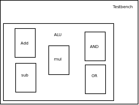
您可以在图像中看到,ALU是顶级实体,包含子模块,它们相互连接或在顶部共享信号。
Testbench具有最高级别的顶层,在这里,、DUT、 (Designed )的实例将被测试(-Design)。
从根本上刺激信号进入DUT并得到同样的响应。
确保您没有从多个模块中驱动相同的信号,就像在您的例子中那样,Y是由ALU的add、sub、mul和OR模块驱动的,需要分离。
删除clk信号,因为组合电路根本不需要clk .
请参阅使用tb的干净代码,如上面提到的那样修改它:
module Add #(parameter BITS=8)(A,B,Y,S,enb);
input wire enb;
input wire [2:0] S;
input wire [BITS - 1:0] A ,B;
output wire [BITS - 1:0] Y;
assign Y = (A + B) & {BITS{enb & (S == 3'b000)}};
endmodule
module Tolak #(parameter BITS=8) (A,B,Y,S,enb);
input enb;
input [2:0] S;
input [BITS - 1:0] A ,B;
output wire [BITS - 1:0] Y;
assign Y = (A - B) & {BITS{enb & (S == 3'b001)}};
endmodule
module Darab #(parameter BITS=8) (A,B,Y,S,enb);
input enb;
input [2:0] S;
input [BITS - 1:0] A ,B;
output wire [BITS - 1:0] Y;
assign Y = (A * B) & {BITS{enb & (S == 3'b010)}}; // truncated to 8 bit only
endmodule
module GateOr #(parameter BITS=8) (A,B,Y,S,enb);
input enb;
input [2:0] S;
input [BITS - 1:0] A ,B;
output wire[BITS - 1:0] Y;
assign Y = (A | B) & {BITS{enb & (S == 3'b011)}}; // truncated to 8 bit only
endmodule
module GateAnd #(parameter BITS=8) (A,B,Y,S,enb);
input enb;
input [2:0] S;
input [BITS - 1:0] A ,B;
output wire [BITS - 1:0] Y;
assign Y = (A & B) & {BITS{enb & (S == 3'b100)}}; // truncated to 8 bit only
endmodule
module Maintb ();
parameter SIZE=8;
reg clk, enb ;
reg [2:0] S;
reg [SIZE -1:0] A,B;
wire [SIZE -1:0] Y,Y1,Y2,Y3,Y4,Y5;
Add #(SIZE) dut (A,B,Y1,S,enb); //000
Tolak #(SIZE) dut1 (A,B,Y2,S,enb); //001
Darab #(SIZE) dut2 (A,B,Y3,S,enb); //010
GateOr #(SIZE) gate (A,B,Y4,S,enb); //011
GateAnd #(SIZE) gate1 (A,B,Y5,S,enb);//100
assign Y = Y1 | Y2 | Y3 | Y4 | Y5;
initial
begin
clk = 1'b0;
enb = 1'b0;
enb = 1'b0; A=8'b0000_0000; B=8'b0001_0000; S=3'b000;
end
// generate clock
always #10 clk = ~clk;
initial
begin
@(posedge clk);
@(posedge clk);
@(posedge clk);
@(posedge clk);
@(posedge clk); enb = 1'b1; A=8'b0000_0001; B=8'b0000_0010; S=3'b000; //add
@(posedge clk); enb = 1'b0;
@(posedge clk); enb = 1'b1; A=8'b0000_0011; B=8'b0010_0000; S=3'b001; //tolak
@(posedge clk); enb = 1'b0;
@(posedge clk); enb = 1'b1; A=8'b0000_1001; B=8'b0000_0000; S=3'b010; //darab
@(posedge clk); enb = 1'b0;
@(posedge clk); enb = 1'b1; A=8'b0010_0001; B=8'b0100_0000; S=3'b011; //or
@(posedge clk); enb = 1'b0;
@(posedge clk); enb = 1'b1; A=8'b1000_0001; B=8'b0000_0000; S=3'b100; //and
@(posedge clk); enb = 1'b0;
@(posedge clk); enb = 1'b0; A=8'b0000_0000; B=8'b0001_0000; S=3'b000; //and
#100 $finish;
end
initial
begin
$monitor("clk %b A-%b B-%b Y-%b S-%b enb-%b",clk, A, B, Y, S, enb);
end
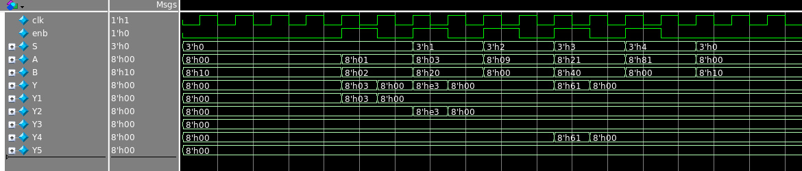
endmodule模拟:
Stack Overflow用户
发布于 2016-05-24 12:57:47
首先,模块GateOr和GateAnd将在它们的S信号中有非法范围.
input [BITS - 14:0] S;与位=8使它..。好吧,-6:0除此之外,您正在将所有输出同时驱动到Y。,并且考虑到您正在执行逻辑-或,而不是a,并且,在您的模块中,所有这些都将同时处于活动状态。
很抱歉,你的设计完全错了。您应该使每个子块时钟独立(使用always @(*)块而不是时钟驱动的块),然后在顶层模块中实例化所有这些子块,每个子块的输出都被驱动到Y_Add、Y_Tolak、Y_Darab、Y_GateOr和Y_GateAnd信号。最后,在顶层,您可以有一个时钟块,其内容如下:
always @(posedge clk)
begin:
  if (enb == 1'b1):
    case (S)
      3'b000: Y <= Y_Add;
      3'b001: Y <= Y_Tolak;
      [...]
    endcase
end并确保Y是reg,而不是wire。基本上,您将使用从多路复用器驱动的值来实现寄存器。
https://stackoverflow.com/questions/37410857
复制相似问题
腾讯云开发者

Copyright © 2013 - 2026 Tencent Cloud. All Rights Reserved. 腾讯云 版权所有
深圳市腾讯计算机系统有限公司 ICP备案/许可证号:粤B2-20090059 ![]() 粤公网安备44030502008569号
粤公网安备44030502008569号
腾讯云计算(北京)有限责任公司 京ICP证150476号 | 京ICP备11018762号