
如何解决KiCad中的足迹丢失错误
如何解决KiCad中的足迹丢失错误
提问于 2020-03-28 09:23:40
我是KiCad的新手。当我在PCB中创建一个netlist时。它显示了这个错误:
错误:没有为符号“R1”定义占用空间。错误:没有为符号“C1”定义占用空间。错误:由于缺少占用空间,无法添加新符号C1
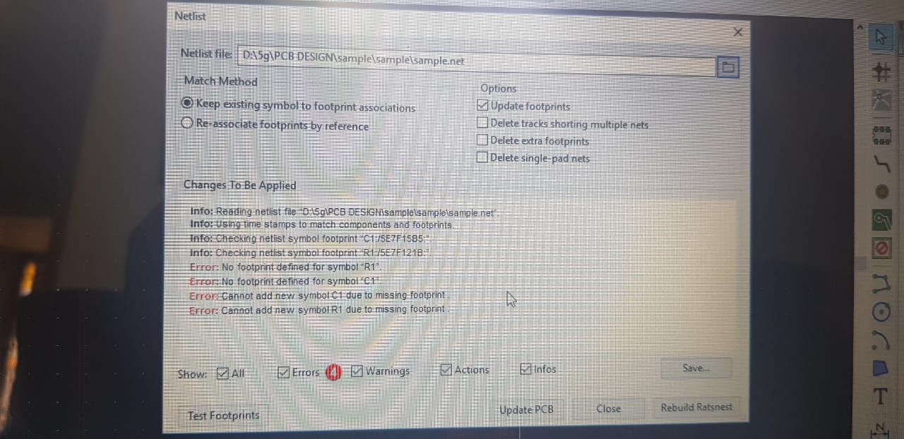
错误:由于缺少占用空间,无法添加新符号R1。
帮我解决这个问题。
回答 1
Stack Overflow用户
发布于 2020-04-01 21:19:22
这很奇怪,但是尝试手工添加官方电阻足迹库。我为你找到了这些:smd (表面贴装)和那 (通孔)。下面是你对它们的处理方法:
    1) click and download those archives
    2) extract those files (i recommend you make
    separate directory for footprint and schematic libraries). Upon
    extracting you should end up with two .pretty files (.pretty stands
    for footprint library)
    3) go to kicad
    4) go to pcbnew
    5) now to preferences->manage footprint libraries
    (hope those navigation clues make sense for your os and version of kicad)
    6) scroll down and click + sign (add empty row to the table)
    7) now place your cursor in the newly appeared row and click the directory symbol
    (add existing library to the table) file browser will open and you just select
    one of the .pretty files.
    8) repeat step 7 for the second .pretty file
现在,您的kicad现在配备了两个官方电阻足迹库,这是非常不可能的一些电阻足迹将丢失。
页面原文内容由Stack Overflow提供。腾讯云小微IT领域专用引擎提供翻译支持
原文链接:
https://stackoverflow.com/questions/60899344
复制相关文章
相似问题
腾讯云开发者

Copyright © 2013 - 2026 Tencent Cloud. All Rights Reserved. 腾讯云 版权所有
深圳市腾讯计算机系统有限公司 ICP备案/许可证号:粤B2-20090059 ![]() 粤公网安备44030502008569号
粤公网安备44030502008569号
腾讯云计算(北京)有限责任公司 京ICP证150476号 | 京ICP备11018762号